 Skip to content
 More than 3000 square meters of warehouse, with a large stock
Light weight, small size, easy to air delivery
Injection molding department and machining department
24/7 one-on-one engineer service support
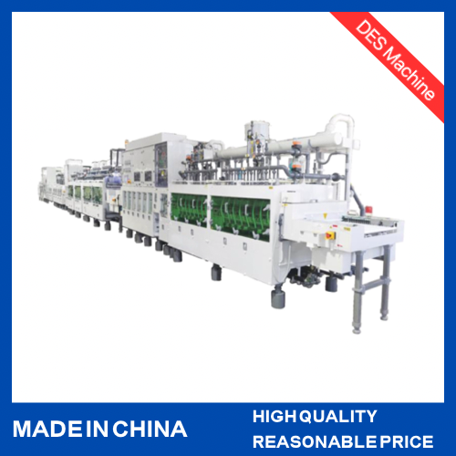
In a PCB (Printed Circuit Board) manufacturing process, the production line typically consists of several stages that involve various equipment for creating the circuit patterns and preparing the board for assembly. Among these, the DES line involve Developing, Etching, and Stripping lines are crucial steps in the process.
Developing of DES LINE:
The developing process occurs after the photolithography stage, where a light-sensitive resist is applied to the PCB. During development, the exposed areas of the resist are washed away, leaving behind a pattern that corresponds to the desired circuit layout. The developing line includes equipment like developing tanks or spray systems that remove the unexposed resist, revealing the copper layers that will be etched.
Etching of DES LINE:
The etching process is used to remove unwanted copper from the PCB, leaving behind the copper traces that form the circuit. The etching line typically includes a chemical etching system (using ferric chloride or other solutions) or a laser etching system. The process follows the developing stage, where the PCB is immersed in the etching solution to dissolve the exposed copper. The etching line ensures the accurate definition of the circuit pattern.
Stripping of DES LINE:
After the etching process, the next step is to remove the remaining photoresist from the PCB. This is done in the stripping line, where chemical solutions or plasma treatment are used to clean off the resist, leaving behind the fully defined copper traces. The stripping process ensures that there are no residues that could interfere with subsequent processes like soldering or testing.
Preparation of PCB Substrate: The PCB substrate is typically made from materials like FR4 (fiberglass) or other composites, with a thin layer of copper foil laminated onto it.
Inkjet or Laser Direct Imaging (LDI) System: In the DES line, a direct imaging system (either inkjet or laser-based) is used to apply a protective resist material directly onto the copper surface. Unlike traditional photolithography, there’s no need for a photomask.
Resist Application: After the resist is applied, the PCB is baked to ensure proper adhesion of the resist material to the copper surface.
Etching Process: The PCB is then exposed to an etching solution, usually a mixture of acids (such as ferric chloride or ammonium persulfate), which dissolves the copper not protected by the resist.
Resist Removal (Striping): After etching, the resist material, which protected the copper areas, is removed in a process called resist stripping.
Inspection and Quality Control: The etched PCB is inspected for quality assurance to ensure the copper traces are accurately formed and free from defects such as under-etching or over-etching.
Cleaning and Final Rinsing: Once the resist has been stripped and the board inspected, the PCB is thoroughly cleaned and rinsed to remove any remaining chemicals or residues from the etching and resist removal steps.
Final Process (Plating, Soldermask, and Surface Finish): After the direct etching process, the PCB may undergo additional steps such as electroplating to add a layer of copper for vias or other features, soldermask application, and surface finish for protection and enhanced solderability.
This occurs when the photoresist is not properly developed, leaving some areas underexposed or overexposed.
Solution: Ensure proper exposure time and uniformity of the UV light source. Also, check the quality of the developing solution and its temperature to maintain consistency.
This happens when too much photoresist is removed, causing loss of fine details.
Solution: Adjust the development time to the optimal level, and regularly calibrate the developer’s concentration and temperature to prevent over-developing.
If the development time is too short, the photoresist may not fully wash away, causing circuit defects.
Solution: Extend the development time slightly or use a more effective developer. Periodically check the resist film thickness to ensure correct exposure levels.
This can result in circuits with inconsistent trace widths, leading to potential performance issues.
Solution: Ensure the etching solution is uniform and properly agitated. Adjust the temperature and concentration of the etchant to ensure consistent etching across the board.
This occurs when the etching process removes too much copper, damaging the circuit traces or making them too thin.
Solution: Monitor etching time closely and calibrate the etching machine. Also, check for proper rinsing to avoid any residual chemicals causing further etching after the process.
If the etching solution is not strong enough or the time is insufficient, some copper may remain on the PCB, affecting circuit performance.
Solution: Increase the etching time slightly or adjust the solution concentration. Regularly inspect the PCB to ensure complete etching before moving to the next step.
If the photoresist isn’t fully removed, it can interfere with subsequent processes, like soldering.
Solution: Use the correct stripper solution and ensure it’s at the proper temperature and concentration. Check the PCB thoroughly for any remaining resist after the process.
Aggressive stripping chemicals or techniques can damage the copper traces or underlying PCB layers.
Solution: Use milder stripping solutions and avoid prolonged exposure to harsh chemicals. Perform gentle stripping techniques to protect the PCB structure.
Incomplete removal of stripper chemicals can cause contamination in the final product.
Solution: Thoroughly rinse the PCB after stripping to ensure all chemicals are removed. Implement a quality control check to verify the cleanliness of the board before moving to the next stage.
Match production requirements with DES line specifications
Production requirements: Ensure that the production capacity of the equipment meets your production requirements. For example, some devices may be suitable for small series production, while others are designed for mass production.
Board size and thickness: Select a device that fits the size and thickness range of the boards you produce. The carrying capacity of different equipment varies, so make sure the equipment is adapted to your actual needs.
Process compatibility of DES line
Technical support: Check whether the equipment can support the process you need, especially for special requirements during etching and development, such as chemical types, temperature control, etc.
Degree of automation: Choose the right level of automation. If your production requires high efficiency and precision, a highly automated device may be more suitable, reducing manual intervention and improving production efficiency and consistency.
DES line quality and stability
Reliability: The stability of the equipment directly affects the production efficiency and product quality, so it is necessary to understand the quality standards and after-sales service of the equipment before purchase. It is best to choose the brand with good reputation in the market.
Equipment accuracy: Especially in the etching and development process, accuracy is very important to ensure that the equipment can maintain high-precision processing capabilities to meet the high requirements of the circuit board.
Chemical and environmental compatibility
Chemical consumption: Understand the types and consumption of chemicals required in each process. For example, specific chemical solutions may be required during etching, and it is important to understand their lifetime and replacement cycle.
Waste treatment: Whether the waste treatment system of the equipment is perfect, in line with local environmental protection requirements, to avoid affecting production due to wastewater and exhaust gas emissions.
DES line maintenance and maintenance
Easy maintenance: Equipment design should take into account daily maintenance, easy to clean, maintain and replace parts. The operation and maintenance manual of the equipment should be perfected, and it is best to choose a supplier with mature after-sales support.
Spare parts supply: Understand whether the equipment manufacturer can provide timely spare parts supply and technical support to reduce equipment downtime.
Cost and budget
Equipment procurement costs: In addition to initial procurement costs, long-term operating costs, maintenance costs and consumables costs should be taken into account.
Long-term return on investment: Whether the quality and performance of the equipment can improve production efficiency and reduce failure rates, ensuring that it can bring long-term return on investment.
Production site and installation requirements
Space requirements: Prepare production line space according to the size and layout requirements of the equipment. Whether special environmental conditions, such as power and ventilation, are required for the installation and commissioning of the equipment.
Transportation and installation: When selecting a supplier, find out about the transportation and installation services of the equipment and whether these services are included in the quotation.
Technical support and training
Supplier support: Ensure that suppliers provide technical support, training, and professional training in equipment operation and maintenance to help your technicians quickly master equipment operation.
Software and system integration: Some equipment may need to be integrated with existing production management systems to ensure that the software provided by the equipment is compatible with your system.
102, No.14-1 Jixiang 3rd Road, Yixin Community, Longgang District, Shenzhen, Guangdong Province, China.
+ 86 181 8840 4906
eternal02023@gmail.com
We’re professional manufacturer of PCB equipment and consumable. We can give you the best advice for your requirements.
© All Rights Reserved.
WhatsApp us
Eternal Tech is committed to becoming an expert in PCB conveying systems.
 Optimized by Seraphinite Accelerator