 Skip to content
 More than 3000 square meters of warehouse, with a large stock
Light weight, small size, easy to air delivery
Injection molding department and machining department
24/7 one-on-one engineer service support
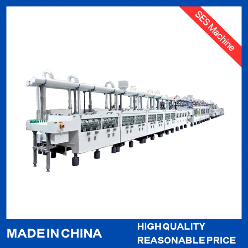
PCB developing machine refers to the process and stages involved in the creation of a printed circuit board (PCB) during its manufacturing process. Specifically, “development” in PCB manufacturing typically refers to the photolithographic steps where the design or pattern of the circuit is transferred onto the copper layer of the board.
Developer Tank of PCB Developing Machine: The developer tank holds the developing solution that is used to remove the unexposed photoresist from the board after exposure. The photoresist that was exposed to UV light hardens, while the unexposed part remains soft and is washed away.
Conveyor System of PCB Developing Machine: A conveyor system moves the PCB through the various stages of the developing process. It ensures smooth transport of the board from one station to another, often at a controlled speed to ensure proper exposure to the developer.
UV Exposure Unit: Before developing, the PCB is exposed to UV light through a photomask. The UV exposure hardens the photoresist in the areas where the pattern is not blocked by the mask, creating the copper traces and insulation areas.
Spray Nozzles or Spray Chambers of PCB Developing Machine: These are used in the developer tank to spray the developing solution evenly across the PCB, ensuring uniform exposure of the board surface to the chemical solution.
Rinsing Station of PCB Developing Machine: After the developing process, the PCB is usually rinsed with water or another cleaning solution to remove any residual chemicals and to stop the developing process.
Drying System of PCB Developing Machine: After the developing and rinsing stages, the PCB is dried, often using hot air or an infrared drying system to remove any moisture from the surface before the next steps in the PCB manufacturing process.
Inspection System of PCB Developing Machine: An optical inspection system might be included to check the developed PCB for defects, ensuring that the photoresist was properly removed and the pattern is correct.
Preparation of the PCB
The PCB is first cleaned to remove any dirt or contaminants.
A thin layer of copper is then applied to the surface of the board. This copper layer will eventually form the conductive paths for the circuit.
Photoresist Application
A photoresist layer is applied to the copper surface. This resist material is sensitive to ultraviolet (UV) light.
The photoresist layer is then exposed to UV light through a mask that contains the desired circuit pattern.
Exposure
The PCB is exposed to UV light through the photomask, which hardens the photoresist material that is directly exposed to the light. The areas that are not exposed to light remain soft and can be washed away in the next step.
Development
The board is then placed in a developer solution, which dissolves the unexposed (soft) photoresist. This reveals the copper areas that were not protected by the resist layer.
The developed areas will form the traces of the PCB, while the remaining copper areas will be removed in the next etching step.
Etching
The exposed copper is then removed by an etching solution, typically a mixture of acid or other chemical etchants. The remaining copper, protected by the hardened photoresist, forms the traces that will carry electrical signals.
After etching, the remaining photoresist is stripped off, leaving behind the finished copper traces.
Inspection and Testing
After development, the PCB is inspected for any defects, such as broken traces or misaligned patterns. Testing is also done to ensure the integrity of the traces before moving on to further manufacturing steps.
Uneven development can lead to the exposure of unwanted areas, or overdevelopment can cause excessive removal of the photoresist, affecting the circuit pattern.
Solution: Ensure uniform exposure during the photolithography process. Adjust the development time and ensure the developer solution is fresh. Maintain a consistent temperature for the developer to avoid overdevelopment.
Underdevelopment results in incomplete removal of the photoresist in certain areas, leading to poor etching or open circuits.
Solution: Check the exposure parameters (time, light intensity, and alignment). Use the appropriate development time and agitation to ensure proper resist removal. Inspect the PCB under a microscope to verify uniform development.
Development marks or lines may appear on the surface of the PCB, which are often caused by poor contact with the development solution or uneven exposure.
Solution: Use a more consistent and gentle agitation technique during development. Ensure that the PCB is properly immersed in the developer solution. Adjust the exposure time to prevent overexposure.
Incomplete or inconsistent removal of the photoresist can lead to poor quality of the PCB’s conductive paths.
Solution: Use appropriate solvents for resist stripping. Consider using a chemical stripper that is suitable for the specific photoresist type. Ensure the resist stripping process is carefully controlled, both in terms of temperature and timing.
The lines or patterns on the PCB are too broad or blurry, often due to poor resolution in the photolithography step.
Solution:Use a higher-resolution photomask. Adjust exposure parameters like time, intensity, and focus to achieve better pattern definition. Ensure that the photomask is properly aligned during the exposure process.
The photoresist may adhere to the development tray or surface during development, leading to residue or contamination on the PCB.
Solution: Use anti-static or non-stick trays. Ensure proper agitation and chemical treatment to reduce resist adhesion. Regularly clean trays to avoid buildup of residues.
Line Width and Spacing of PCB Developing Machine: Ensure that the width of the traces and the spacing between them comply with the manufacturing process and design requirements. Narrow traces and small spacings can lead to signal integrity problems or manufacturing defects.
Signal Integrity of PCB Developing Machine: For high-speed signals, ensure the development line layout minimizes impedance mismatches, crosstalk, and noise. Using controlled impedance lines or differential pair routing can help.
Thermal Management of PCB Developing Machine: If the PCB will carry high current, ensure the traces are wide enough to prevent excessive heat buildup, which could damage the PCB.
Current Carrying Capacity of PCB Developing Machine: Ensure the width of the trace is sufficient to carry the required current without excessive voltage drop or overheating. There are standards and calculators available to determine appropriate trace widths based on the current.
Manufacturing Capabilities: Ensure the selected trace width and spacing are achievable with the chosen PCB manufacturer’s capabilities. Some manufacturers have limitations on the minimum trace width and spacing they can produce.
DFM (Design for Manufacturability): Consider the impact of the trace design on the manufacturability of the PCB. Complex or very fine traces may increase the risk of defects during production.
Soldering and Reliability: Ensure that the traces are designed in a way that allows for easy soldering without causing shorts or reliability issues during the assembly process.
Environmental Considerations: For PCBs that will be exposed to harsh conditions (e.g., high temperatures, humidity, or chemicals), select traces and materials that can withstand such environments.
Testability: Design traces in a way that they can be easily tested for electrical continuity and quality during production.
102, No.14-1 Jixiang 3rd Road, Yixin Community, Longgang District, Shenzhen, Guangdong Province, China.
+ 86 181 8840 4906
eternal02023@gmail.com
We’re professional manufacturer of PCB equipment and consumable. We can give you the best advice for your requirements.
© All Rights Reserved.
WhatsApp us
Eternal Tech is committed to becoming an expert in PCB conveying systems.
 Optimized by Seraphinite Accelerator